STM32-PCB
STM32F411CEU6 Development Board with Integrated IMU and High-Speed USB Interface
Overview
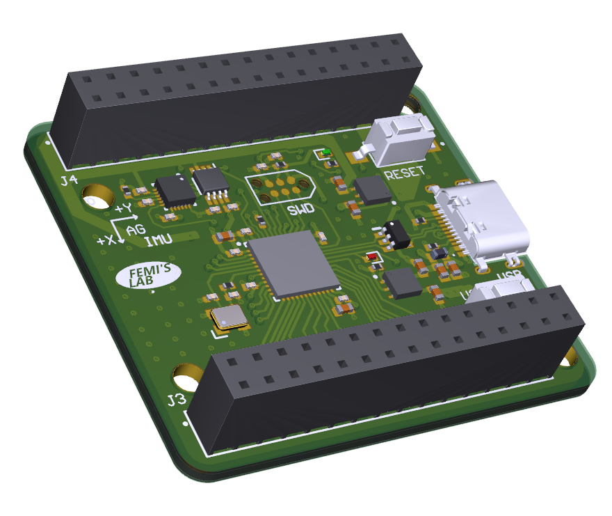
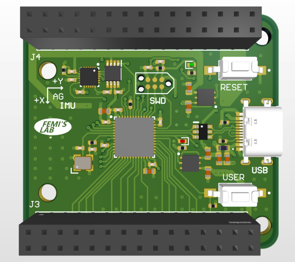
I designed a custom four-layer STM32F411CEU6-based development board incorporating an Inertial Measurement Unit (IMU) and a high-speed USB interface. This board provides a versatile platform for embedded systems development, focusing on signal integrity, sensor integration, real-time processing, and rapid prototyping.
Features:
Microcontroller: STM32F411CEU6 for high-performance processing and low power consumption.
Integrated IMU: The board features an onboard ICM20948 9-DoF accelerometer, gyroscope, and magnetometer for motion sensing, ideal for wearables, robotics, and navigation systems.
USB Connectivity: A high-speed USB interface for fast data communication and powering the device.
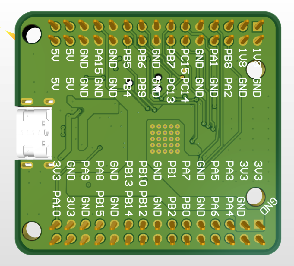
Headers: Easily accessible GPIO headers for interfacing with external devices and sensors.
SWD Interface: A tag connect serial wire debugging interface for easy programming and development.
Achievements and Learning Outcomes:
Component Selection: I researched and selected each component based on performance requirements, availability, price, and compatibility with the STM32 microcontroller.
Schematic Layout Design: Creating the schematic for this design involved organizing the various subsystems—microcontroller, IMU, power management, and USB interface—while ensuring proper signal routing and power distribution.
Component Placement and PCB Design: I carefully placed components to minimize signal interference and optimize board space. This was crucial in a compact design where noise-sensitive components like the IMU and clock sources need isolation from noisy digital signals. I gave special attention to the placement of the USB connector to ensure easy and reliable differential pair routing.
Controlled Impedance Routing: High-speed signals, such as USB data lines, require controlled impedance traces. I calculated the trace widths and spacing according to the layer stack up to maintain signal integrity and reduce noise.
Layer Stack Management: The board's four-layer stack consists of signal layers, a ground plane, and a polygon power distribution. This configuration ensured low electromagnetic interference (EMI), signal integrity, and efficient power distribution.
Design for Manufacturing and Testing (DFM/DFT): Throughout the design, I considered manufacturability by ensuring proper clearances, pad sizes, and via types to facilitate both manual and automated assembly. I also included test points and easy access to critical signals for post-assembly testing.
Conclusion
This project allowed me to build expertise in various aspects of PCB design, from component selection to manufacturing considerations. The integration of high-speed USB, an IMU, and the STM32 microcontroller in a compact form factor is significant in my development as a hardware engineer.
Project information
- Category PCB Design
- Client Personal
- Project date June, 2024
- PCB 3D Model Please use Adobe Acrobat Reader
- Project URL https://github.com/iamflinks/STM32-PCB
- Visit Website